Popular posts from this blog
VLSI: 4-1 MUX Dataflow Modelling with Testbench
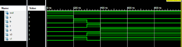
Verilog Code for 4-1 MUX Dataflow Modelling module m41(out, i0, i1, i2, i3, s0, s1); output out; input i0, i1, i2, i3, s0, s1; assign y0 = (i0 & (~s0) & (~s1)); assign y1 = (i1 & (~s0) & s1); assign y2 = (i2 & s0 & (~s1)); assign y3 = (i3 & s0 & s1); assign out = (y0 | y1 | y2 | y3); endmodule //Testbench code for 4-1 MUX Dataflow Modelling initial begin // Initialize Inputs a = 1;b = 0;c = 0;d = 0;s0 = 0;s1 = 0; ...
Samir Palnitkar Solution Manual Free Download PDF of Verilog HDL

This is a solution guide to the exercises of the book "The Solution Manual of the Verilog HDL: A Guide to Digital Design and Synthesis by Samir Palnitkar". Following are the Solutions to Solution Manual on Verilog HDL: A Guide to Digital Design and Synthesis by Samir Palnitkar , exercises of all chapters in the book. Chapter 1 ----------------- No Exercises ---------------- Chapter 2 : Hierarchical Modeling Concepts Chapter 3 : Basic Concepts Chapter 4 : Modules and Ports Chapter 5: Gate-level Modeling Chapter 6 : Dataflow Modeling Chapter 7 : Behavioral Modeling Chapter 8 : Tasks and Functions Download Solution Manual: Click on this link (Mega.nz Link) [Solution Manual to Verilog HDL: A Guide to Digital Design and Synthesis by Samir Palnitkar] Preview of Solution Manual: For Verilog Programs: Go to Index of Verilog Programming Tags: Verilog HDL solutio...
Verilog: 4 Bit Counter Behavioral Modelling using If Else Statement

Verilog Code for 4 Bit Counter Behavioral Modelling using If Else Statement module 4_bit_Count( input clock, reset, output [3:0]dout ); reg [3:0]dout; initial dout = 0; always @ (posedge (clock)) begin if (reset) dout <= 0; else dout <= dout + 1; end endmodule Xillinx Output: 4 Bit Counter Behavioral Modelling Response Also See: List of Verilog Programs
Verilog: 1to 8 DeMultiplexer (1-8 DEMUX) Dataflow Modelling with Testbench Code
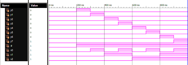
Verilog Code for 1 to 8 DeMultiplexer Dataflow Modelling module demux_1_to_8( input d, input s0, input s1, input s2, output y0, output y1, output y2, output y3, output y4, output y5, output y6, output y7 ); assign s0n = ~ s0; assign s1n = ~ s1; assign s2n = ~ s2; assign y0 = d & s0n & s1n & s2n; assign y1 = d & s0 & s1n & s2n; assign y2 = d & s0n & s1 & s2n; assign y3 = d & s0 & s1 & s2n; assign y4 = d & s0n & s1n & s2; assign y5 = d & s0 & s1n & s2; assign y6 = d & s0n & s1 & s2; assign y7 = d & s0 & s1 & s2; endmodule //Testbench code for 1-8 DEMUX Dataflow Modelling initial begin // Initialize Inputs d = 0;s0 = 0;s1 = 0;s2 = 0; // Wait 100 ns for global reset to finish #100; // Add stimulus here #100; d = 1;s0 = 0;s1 = 0;s2 = 0; #100; d = 1;s0 = 1;s1 = 0;s2 = 0; #100; d = 1;s0 = 0;s1 = 1;s2 = 0; #100; d = 1;s0 = 1;s1 = 1;s2 = 0; #100; d = 1;s0 = 0;s1 = 0;s2 = 1; ...
VLSI: 1-4 DEMUX (Demultiplexer) Dataflow Modelling with Testbench

Verilog Code for 1-4 DEMUX Dataflow Modelling module demux_1_to_4( input d, input s0, input s1, output y0, output y1, output y2, output y3 ); assign s1n = ~ s1; assign s0n = ~ s0; assign y0 = d& s0n & s1n; assign y1 = d & s0 & s1n; assign y2 = d & s0n & s1; assign y3 = d & s0 & s1; endmodule //Testbench code for 1-4 DEMUX Dataflow Modelling initial begin // Initialize Inputs ...