Posts
VLSI: AND Gate Dataflow Modelling with Testbench

Verilog Code for AND gate Dataflow Modelling module ANDgate( input a, input b, output c ); assign c = a & b; endmodule //Testbench code for AND gate Dataflow Modelling initial begin // Initialize Inputs a = 0;b = 0; // Wait 100 ns for global reset to finish #100 a = 0; b = 1; #100 a = 1; b = 0; #100 a = 1; b = 1; e nd Output:
Popular posts from this blog
VLSI: 8-3 Encoder Dataflow Modelling with Testbench
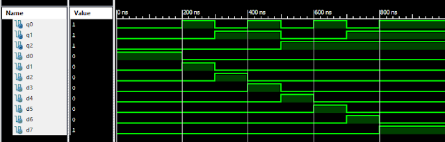
Verilog Code for 8-3 Encoder Dataflow Modelling module encoder_8_to_3( input d0, input d1, input d2, input d3, input d4, input d5, input d6, input d7, output q0, output q1, output q2 ); assign q0 = ( d1 | d3 | d5 | d7 ); assign q1 = ( d2 | d3 | d6 | d7 ); assign q2 = ( d4 | d6 | d5 | d7 ); endmodule //Testbench code for 8-3 Encoder Dataflow Modelling initial begin ...
VLSI: 4-1 MUX Dataflow Modelling with Testbench
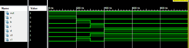
Verilog Code for 4-1 MUX Dataflow Modelling module m41(out, i0, i1, i2, i3, s0, s1); output out; input i0, i1, i2, i3, s0, s1; assign y0 = (i0 & (~s0) & (~s1)); assign y1 = (i1 & (~s0) & s1); assign y2 = (i2 & s0 & (~s1)); assign y3 = (i3 & s0 & s1); assign out = (y0 | y1 | y2 | y3); endmodule //Testbench code for 4-1 MUX Dataflow Modelling initial begin // Initialize Inputs a = 1;b = 0;c = 0;d = 0;s0 = 0;s1 = 0; ...
Verilog: 8 to 1 Multiplexer (8-1 MUX) Dataflow Modelling with Testbench Code
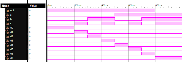
Verilog Code for 8 to 1 Multiplexer Dataflow Modelling module mux_8to1( input a, input b, input c, input D0, input D1, input D2, input D3, input D4, input D5, input D6, input D7, output out, ); module m81( output out, input D0, D1, D2, D3, D4, D5, D6, D7, S0, S1, S2); assign S1bar=~S1; assign S0bar=~S0; assign S2bar=~S2; assign out = (D0 & S2bar & S1bar & S0bar) | (D1 & S2bar & S1bar & S0) | (D2 & S2bar & S1 & S0bar) + (D3 & S2bar & S1 & S0) + (D4 & S2 & S1bar & S0bar) + (D5 & S2 & S1bar & S0) + (D6 & S2 & S1 & S0bar) + (D7 & S2 & S1 & S0); endmodule //Testbench code for 8-1 MUX Dataflow Modelling initial begin // Initialize Inputs a= 0;b = 0;c = 0;D0 = 1;D1 = 0;D2 = 0;D3 = 0;D4 = 0;D5 = 0;D6 = 0;D7 = 0; // Wait 100 ns for global reset to finish #100; // Add stimulus here #100; a = 0;b = 0;c = 1;d0 = ...
VLSI: 1-4 DEMUX (Demultiplexer) Dataflow Modelling with Testbench

Verilog Code for 1-4 DEMUX Dataflow Modelling module demux_1_to_4( input d, input s0, input s1, output y0, output y1, output y2, output y3 ); assign s1n = ~ s1; assign s0n = ~ s0; assign y0 = d& s0n & s1n; assign y1 = d & s0 & s1n; assign y2 = d & s0n & s1; assign y3 = d & s0 & s1; endmodule //Testbench code for 1-4 DEMUX Dataflow Modelling initial begin // Initialize Inputs ...
Verilog: Binary to Gray Converter Structural/Gate Level Modelling with Testbench
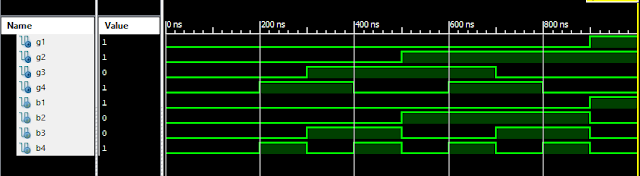
Verilog Code for Binary to Gray Structural/Gate Level Modelling module binary_to_gray( input b1, input b2, input b3, input b4, output g1, output g2, output g3, output g4 ); buf(g1,b1); xor (g2,b1,b2),(g3,b2,b3),(g4,b3,b4); endmodule //Testbench code for Binary to Gray Structural/Gate Level Modelling initial begin // Initialize Inputs b1 = 0;b2 = 0;b3 = 0;b4 = 0; // Wait 100 ns for global reset to finish #100; // Add stimulus here #100;b1 = 0;b2 = 0;b3 = 0;b4 = 1; #100;b1 = 0;b2 = 0;b3 = 1;b4 = 0; #100;b1 = 0;b2 = 0;b3 = 1;b4 = 1; #100;b1 = 0;b2 = 1;b3 = 0;b4 = 0; #100;b1 = 0;b2 = 1;b3 = 0;b4 = 1; #100;b1 = 0;b2 = 1;b3 = 1;b4 = 0; #100;b1 = 0;b2 = 1;b3 = 1;b4 = 1; #100;b1 = 1;b2 = 0;b3 = 0;b4 =...